
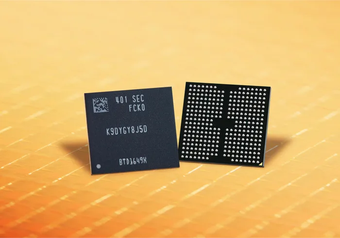
Samsung has implemented the world’s first 900 layer class V-NAND prototype technology. By combining two 450-layer cell wafers with Cell Multi Bonding technology, the company passed an important production threshold on the way to the 1000-layer NAND era. Samsung is approaching the 1000-layer NAND era. Samsung became the first company to increase the number of layers to the 900 class in NAND memory technology. The South Korea-based manufacturer has made its new V-NAND prototype operational with Cell Multi Bonding technology, which combines two 450-layer cell wafers in a single structure.
According to industry sources, normal cell operating characteristics have been confirmed in the system. NAND flash memories are among the key components for artificial intelligence servers, smartphones and data center SSDs. Increasing the number of layers on the V-NAND side provides higher capacity in the same chip area. This structure plays a critical role in terms of storage density and power efficiency. Samsung’s new prototype is positioned at a different level from existing solutions in mass production.
One of the highest layer mass production solutions on the market today is SK hynix’s 321-layer 4D NAND technology. Samsung, on the other hand, is 10th. While it was carrying out production preparations on 400 layers for the next generation V-NAND, that is, V10 platform, it reached 900 layer class in the research phase. Samsung was the first company to commercialize 3D V-NAND technology in 2013. The single-batch production approach used in the early periods faced physical limits as the number of layers increased.
In particular, wafer bending and alignment errors were among the biggest technical problems in high-layer NAND production. Cell Multi Bonding technology used in the 900-layer structure is based on combining two separate 450-layer cell wafers instead of producing a very high NAND tower in one piece. In this process, Samsung solved the wafer bending problem with an advanced top plate design. It also used its own overlay correction technology for micron-level alignment errors that occurred during bonding.
In the new structure, changes were also made to the bit line and word line. According to the information conveyed in the news, Samsung achieved results that reduced both power consumption and chip size thanks to the new BL and WL architecture. This detail shows that the 900-layer structure is considered not only in terms of the number of layers, but also in terms of production efficiency and energy consumption. Competition in the NAND market is not only among South Korean manufacturers.
China-based Yangtze Memory Technologies, or YMTC, is among the companies approaching the 300-layer-class NAND production threshold. Chinese manufacturers are increasing their NAND production capacity and layer technology with government support and local equipment investments. If YMTC switches to NAND production of more than 300 layers within the year, price competition in the NAND market is expected to become tougher.
This chart positions Samsung’s 900-layer class prototype not only as a technical achievement, but also as a long-term technology barrier against capacity and price pressure from Chinese manufacturers. Industry sources state that the 900-layer NAND structure is not just a tripling of 300-layer manufacturing, but a threshold that changes the manufacturing approach. Samsung’s method of combining two 450-layer wafers in a single structure also forms the direct basis for 1000-layer class NAND technology.


Comments
You can write your views about this story. Comments may be moderated according to site settings.