
Computer chips are everywhere, but most people never see how they are made.
They power phones, laptops, cars, smartwatches, game consoles, AI servers and almost every modern device. A chip may look like a small square of material, but inside it are billions of tiny electronic structures built through one of the most precise manufacturing processes in the world.
ASML explains that microchips are made by building layers of interconnected patterns on a silicon wafer. The full manufacturing process involves hundreds of steps and can take up to four months from design to mass production.
That sounds complicated, and it is. But the basic idea is simple: chipmakers start with silicon, create tiny circuit patterns on it, repeat that process many times and then cut, package and test the finished chips.
It starts with silicon
Most computer chips begin with silicon.
Silicon is used because it is a semiconductor, meaning it can behave like a conductor or an insulator depending on how it is treated. That makes it ideal for building transistors, the tiny switches that allow chips to process information.
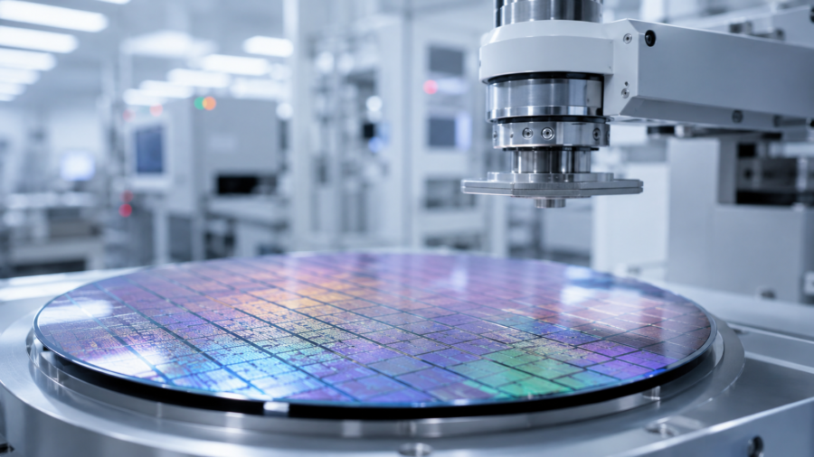
The silicon is formed into a large cylinder called an ingot. That ingot is sliced into thin round discs known as wafers. These wafers are polished until they are extremely smooth.
A single wafer can contain many chips. Instead of making one chip at a time, manufacturers build many copies of the same chip design across the surface of the wafer.
This is one reason chip manufacturing is so powerful but also so difficult. If something goes wrong on a wafer, many chips can be affected at once.
The cleanroom matters
Chip manufacturing happens inside special factories called fabs.
Inside a fab, wafers move through cleanrooms where air quality, humidity and temperature are tightly controlled. ASML notes that robots transport wafers from machine to machine inside these controlled environments.
Cleanrooms are necessary because chip features are extremely small. Dust, vibration or tiny contamination can damage the patterns being created.
For ordinary readers, the easiest way to understand this is to imagine printing a city map on a surface smaller than a fingernail. Now imagine that one speck of dust can ruin part of the map. That is why the factory environment has to be so controlled.
Layers are built one by one
A chip is not made in a single step.
It is built layer by layer. Each layer adds part of the final structure, such as transistor features, insulating materials or metal connections.
ASML describes microchips as complex patterns of transistors built layer by layer on a silicon wafer. OECD also describes semiconductor fabrication as a repeated cycle that can include polishing, deposition, resist application, lithography, etching, ion implantation and resist removal.
That cycle may happen many times. Each repetition adds detail to the chip.
This is why chip manufacturing takes so long. It is not one machine stamping a chip into existence. It is a chain of precise steps repeated again and again.
Lithography prints the tiny patterns
Lithography is one of the most important steps in chip making.
Synopsys defines lithography as a foundational semiconductor manufacturing process used to transfer intricate patterns onto silicon wafers to form integrated circuits. In simple terms, lithography uses light to print tiny circuit patterns onto the wafer.
The wafer is coated with a light-sensitive material called photoresist. A pattern is projected through a mask, and the light changes the exposed parts of the photoresist. After development, that pattern guides the next manufacturing step.
This is how chipmakers create the incredibly small shapes needed for transistors and connections.
Advanced chips often require advanced lithography tools. EUV lithography, or extreme ultraviolet lithography, uses very short-wavelength light to create extremely small patterns. That is why EUV is important for leading-edge processors used in AI, smartphones and high-performance computing.
Etching removes material
After lithography creates a pattern, etching helps carve that pattern into the wafer.
Etching removes selected material from the wafer surface. The photoresist acts like a protective guide, allowing some areas to remain while other areas are removed.
This is similar in concept to using a stencil, though at a microscopic scale. The pattern determines where material stays and where it goes.
Etching must be extremely accurate. If too much material is removed, the chip may not work. If too little is removed, the pattern may not form correctly.
Deposition adds new material
Chipmakers also need to add materials.
Deposition is the process of placing thin films of material onto the wafer. ASML explains that conducting, insulating or semiconducting materials may be deposited depending on what structure is being made.
These layers help form transistors, insulators and electrical connections. Some layers control how current moves. Others separate parts of the chip so signals do not interfere with each other.
The combination of deposition, lithography and etching is central to chip manufacturing. One step adds material, another prints a pattern and another removes selected areas.
Repeated many times, those steps create the tiny structures inside a modern chip.
Doping changes how silicon behaves
Silicon alone is not enough.
To make transistors work, chipmakers must change how certain areas of silicon conduct electricity. This is done through a process often called doping or ion implantation.
In simple terms, tiny amounts of other elements are introduced into the silicon. This changes its electrical behavior and helps create regions that can control current.
This is one reason semiconductors are so useful. Their behavior can be carefully adjusted.
A transistor depends on this control. It can act like a switch, turning signals on or off. Billions of those switches working together allow a chip to process data.
Metal connections link everything together
Once the transistor structures are formed, the chip still needs wiring.
Tiny metal connections are built above the transistor layers to connect different parts of the chip. These connections allow signals and power to move through the circuit.
This part of the process is sometimes called interconnect formation. It is like building roads and bridges between tiny electronic neighborhoods.
Without these connections, the transistors would be isolated. With them, the chip becomes a working electronic system.
Modern chips can have many layers of interconnects. The more complex the chip, the more carefully these connections must be designed and manufactured.
The wafer is tested, cut and packaged
After the wafer is processed, the chips on it must be tested.
Not every chip on a wafer works perfectly. Manufacturing is extremely precise, but defects can still happen. Testing helps identify which chips meet the required standard.
The wafer is then cut into individual pieces called dies. Each die can become one chip.
Those dies are placed into packages. Packaging protects the chip and connects it to the outside world, allowing it to be mounted in phones, laptops, servers or other devices.
Packaging has become more important as chips grow more advanced. Some modern processors combine multiple chiplets or memory components in one package to improve performance.
Why this matters for AI chips
AI chips need enormous computing power.
That power depends on advanced chip design, dense transistor layouts, fast memory and efficient manufacturing. Lithography, etching, deposition and packaging all play a role.
When people talk about AI chips, they often mention companies like NVIDIA, AMD, Apple, Intel, TSMC or Samsung. But behind those names is a long manufacturing chain.
A powerful AI chip is not just designed. It must be manufactured with extreme precision.
That is why chip-making equipment, cleanrooms, wafers and lithography machines are so important to the AI boom. Better manufacturing helps create faster and more efficient processors, which can support larger AI models and more capable devices.
Why chips are hard to make
Computer chips are difficult to manufacture because everything happens at an extremely small scale.
A modern chip may contain billions of transistors. Each one must be built correctly. The process involves hundreds of steps, and many of those steps must align perfectly with previous layers.
The factories are expensive. The machines are complex. The materials must be pure. The environment must be controlled.
This is why only a small number of companies can make the most advanced chips. It requires deep expertise, huge investment and years of process development.
The bigger takeaway
Computer chips may look simple from the outside, but they are among the most complex products humans make.
They begin as silicon wafers and go through hundreds of carefully controlled steps. Lithography prints tiny patterns. Etching removes selected material. Deposition adds new layers. Doping changes electrical behavior. Metal connections link everything together. Testing and packaging turn the wafer into usable chips.
This hidden process powers almost every modern device.
Phones, laptops, cars, game consoles and AI servers all depend on the same basic idea: tiny electronic switches built with extreme precision on silicon.
So the next time a company announces a faster AI chip or a more efficient laptop processor, the story is not only about design. It is also about the remarkable manufacturing process that makes those chips real.


Comments
You can write your views about this story. Comments may be moderated according to site settings.