
Semiconductor lithography sounds like a difficult engineering term, but the basic idea is easier than it looks.
It is one of the most important steps in chip making. Without lithography, modern processors, AI chips, smartphone chips and laptop chips would not be able to contain billions of tiny transistors.
ASML, one of the most important companies in chip-making equipment, describes lithography as a process that helps build complex transistor patterns layer by layer on a silicon wafer. Synopsys also explains lithography as a foundational semiconductor manufacturing step that transfers intricate patterns onto silicon wafers to form integrated circuits.
In simple terms, lithography is how chipmakers “print” tiny circuit patterns onto the material that becomes a chip.
That makes it critical for the AI boom. AI chips need huge computing power, and that power depends on packing more tiny transistors into advanced processors. Lithography is one of the key reasons chipmakers can keep making those circuits smaller, denser and more efficient.
What semiconductor lithography means
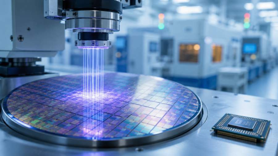
A semiconductor chip begins with a silicon wafer. The wafer is a thin, round slice of silicon that can hold many chips at once.
Lithography helps place extremely small circuit patterns onto that wafer.
The process uses light, a pattern template called a mask or reticle, and a light-sensitive material called photoresist. The wafer is coated with photoresist, then exposed to light through the pattern. After that, the exposed material is developed, and the pattern can be etched into the wafer.
imec explains chip lithography as the transfer of a circuit design onto a silicon wafer using photoresist and light exposure through a mask. That pattern becomes part of the microscopic structure that forms the chip.
This does not happen only once. ASML says the process is repeated many times because chips are built in layers. A modern microchip may require 100 or more patterned layers before the final chip is complete.
That is why lithography is so important. It is not a small side step. It is one of the central processes that allows modern electronics to exist.
Why chip making needs such tiny patterns
A chip works because it contains transistors. A transistor is like a tiny switch that helps process information.
Modern chips need billions of these switches. The smaller and more efficiently they can be arranged, the more powerful and energy-efficient the chip can become.
This is why chipmakers care so much about advanced manufacturing. Smaller patterns can allow more transistors to fit into the same area. That can improve performance, reduce power use and support more complex features.
For everyday users, this shows up in familiar ways. Phones become faster. Laptops become more efficient. Game consoles process better graphics. Data centers run larger AI models. Smart devices can do more without draining as much power.
Lithography is one of the technologies behind those improvements.
What EUV lithography is
EUV stands for extreme ultraviolet.
EUV lithography uses extremely short-wavelength light to print very tiny chip patterns. ASML says EUV light has a wavelength of 13.5 nanometers, much shorter than the deep ultraviolet light used in older lithography systems. Shorter wavelengths help print smaller features on a chip.
This is important because leading-edge chips need extremely fine details. ASML says EUV lithography helps chipmakers pack more and smaller transistors into each new generation of microchips, making them more powerful, faster and more energy efficient.
EUV is not used for every part of every chip. Different layers may use different lithography technologies. ASML explains that chipmakers use newer EUV systems for the smallest features and older DUV systems for larger features.
That matters because advanced chip manufacturing is not one machine doing everything. It is a long sequence of highly precise steps.
Why AI chips depend on advanced lithography
AI chips are designed to handle huge amounts of calculation. Training and running AI models requires massive computing power, fast memory movement and high energy efficiency.
Advanced lithography helps chipmakers create processors that can support those demands.
More transistors can allow more compute units, better acceleration, improved memory systems and more efficient performance. That is why companies building AI hardware care so much about the most advanced semiconductor manufacturing nodes.
ASML says chips made with EUV lithography are enabling artificial intelligence, smart devices, augmented reality and other advanced technologies. In other words, EUV is not only a factory tool. It is part of the hidden infrastructure behind modern AI products.
This is also why AI chip demand affects the wider semiconductor supply chain. TSMC’s CEO recently said the company is working hard to meet strong AI-driven demand and avoid becoming a bottleneck in the chip supply chain. Reuters reported that TSMC is seeing strong demand tied to the AI boom. :contentReference[oaicite:1]{index=1}
For readers, the connection is simple: better AI chips require better manufacturing, and better manufacturing depends heavily on lithography.
Why lithography machines are so expensive
Lithography machines are among the most complex tools in the technology industry.
They need to control light, mirrors, masks, software, wafer movement and extremely precise alignment at microscopic scales. Even tiny errors can ruin a pattern.
EUV systems are especially difficult because EUV light is hard to generate and control. ASML explains that EUV light occurs naturally in outer space, but creating it inside a machine required a radically new approach. The company uses 13.5-nanometer EUV light for advanced lithography. :contentReference[oaicite:2]{index=2}
This complexity is one reason advanced chip-making equipment is so expensive. Recent reporting on TSMC and ASML’s High-NA EUV systems notes that the newest machines can cost hundreds of millions of dollars each, and TSMC is researching the tools while watching costs carefully. :contentReference[oaicite:3]{index=3}
That cost matters because it can affect the economics of advanced chips. If the machines, factories and materials become more expensive, chipmakers must decide when the performance gains are worth the production cost.
Why this matters beyond factories
Most people will never see a lithography machine. But they use the results every day.
Every smartphone, laptop, tablet, game console, smartwatch and AI server depends on semiconductor manufacturing. When chips become more powerful and efficient, consumer devices improve.
Lithography also affects competition. Companies like TSMC, Intel and Samsung Foundry compete to manufacture advanced chips. Equipment suppliers like ASML are central because their machines make the most advanced production possible.
This is why semiconductor lithography appears in discussions about AI, national technology policy, supply chains and future devices. It may sound like a factory process, but it helps shape the technology people use every day.
If lithography advances, future chips can become more capable. If lithography becomes harder or more expensive, progress may slow or become concentrated among fewer companies.
What ordinary readers should take away
Semiconductor lithography is the process that helps print tiny circuit patterns onto silicon wafers.
It is one of the most important steps in chip making because it allows manufacturers to build the dense transistor patterns inside modern processors.
EUV lithography is the advanced version used for some of the smallest and most demanding chip features. It is critical for leading-edge chips used in AI, smartphones, high-performance computing and other advanced technologies.
The reason this matters now is the AI boom. AI systems need powerful chips, and powerful chips depend on advanced manufacturing. Lithography is one of the hidden technologies making that possible.
So when people talk about AI chips, GPU shortages or the cost of future devices, the conversation is not only about NVIDIA, Apple, AMD or Qualcomm. It is also about the tools that make those chips possible.
Semiconductor lithography may happen far away inside cleanrooms, but it plays a direct role in the phones, laptops and AI tools people use every day.


Comments
You can write your views about this story. Comments may be moderated according to site settings.