
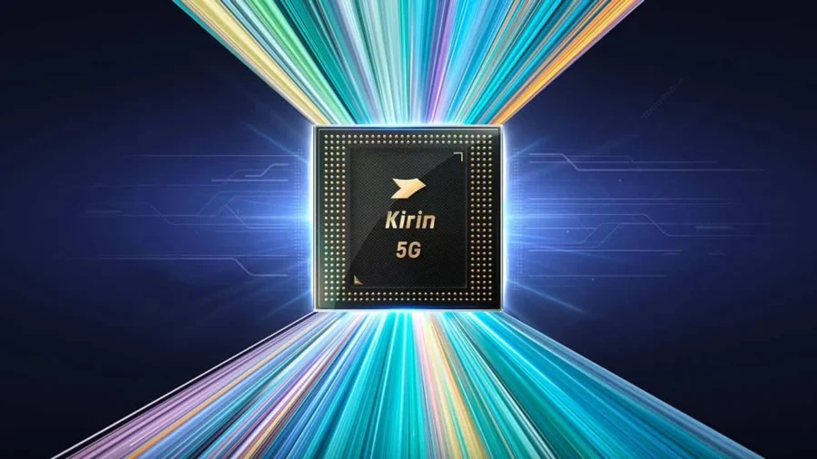
Huawei showed its new road map on the mobile processor side, which does not rely only on smaller production technologies. The Tau scaling approach, which the company shared at the 2026 IEEE International Symposium on Circuits and Systems event, focuses on improving performance, efficiency and transistor density by reducing signal delay in chips. The first major commercial step of this plan will be the new Kirin chips, which will be released in the fall of 2026.
The architecture, which Huawei calls LogicFolding, shortens the critical signal paths inside the processor by moving the traditional single-layer logic layout to a more compact and double-layer structure. Huawei switches to LogicFolding architecture in new Kirin chips. In the framework shared by Huawei, Tau scaling differs from the geometric shrinkage approach based on Moore’s Law. The main idea here is to ensure that the signals inside the chip travel in a shorter time, rather than physically shrinking the transistors.
That’s why LogicFolding architecture is described as a structure that works together at the device, circuit, chip and system level. According to the company’s technical explanation, the resistance and parasitic capacitance values of transistors and connections are reduced at the device level. Critical path cabling is shortened by breaking traditional layout boundaries at the circuit level. At the chip level, software, architecture and silicon sides are handled together.
At the system level, memory addressing and communication delay are rearranged with the connection approach called UnifiedBus. It is stated that the transistor density in Kirin chips released in 2026 will increase by 53.5 percent, reaching approximately 238 million transistors/mm². In the same technical sharing, there is a 41 percent increase for high performance core efficiency and a 12.7 percent increase for the highest clock speed, reaching approximately 3.1 GHz.
On the Huawei side, this transition is conveyed with the assessment that mobile processors have entered a more limited area in terms of performance increase after the Kirin 9030 Pro. At this point, the company draws a picture that shrinking the production node alone is not enough and focuses on architectural regulation in the new Kirin generation. Tau scaling is not a topic limited only to mobile processors. Huawei explains that it has designed and mass produced 381 chips with ideas around this approach in the last six years.
Kirin chips, which will arrive in the fall of 2026, are positioned as the first Kirin family to carry the LogicFolding architecture. The year 2031 draws attention in the further part of the road map. Huawei shares that Tau scaling-based high-end chips can achieve a transistor density of 14 angstroms, equivalent to 1.4 nm class production processes, by 2031. For the same period, density over 400 million transistors/mm² and clock speeds reaching 5.0 GHz are also included in the technical road map.
The important distinction at this point is that the 1.4 nm expression is not presented directly as a physical production process. The approach described by Huawei involves approaching similar density and performance levels through architecture, signal path and system design, without moving to a more advanced production node.


Comments
You can write your views about this story. Comments may be moderated according to site settings.