
NVIDIA has brought forward the optical link schedule for data transfer load in AI data centers, which is at the limit of copper connections. Co-Packaged Optics, or CPO technology, will first enter NVIDIA’s next generation artificial intelligence platforms with the Feynman GPU family in the 2028 calendar. This change means that the company has moved its optical connection roadmap to 2028 instead of 2033. NVIDIA will exceed the copper connection limit with Feynman GPU.
As artificial intelligence systems grow, not only GPU power but also the speed of data flow between these GPUs becomes decisive. In large-scale AI infrastructures, as the distance between servers, racks and platforms increases, traditional copper connections create more latency, power consumption and scaling problems. This is where CPO technology comes into play. The system is based on silicon photonic infrastructure, which carries the signal through light instead of copper, and positions the optical components much closer to the processor or network chips.
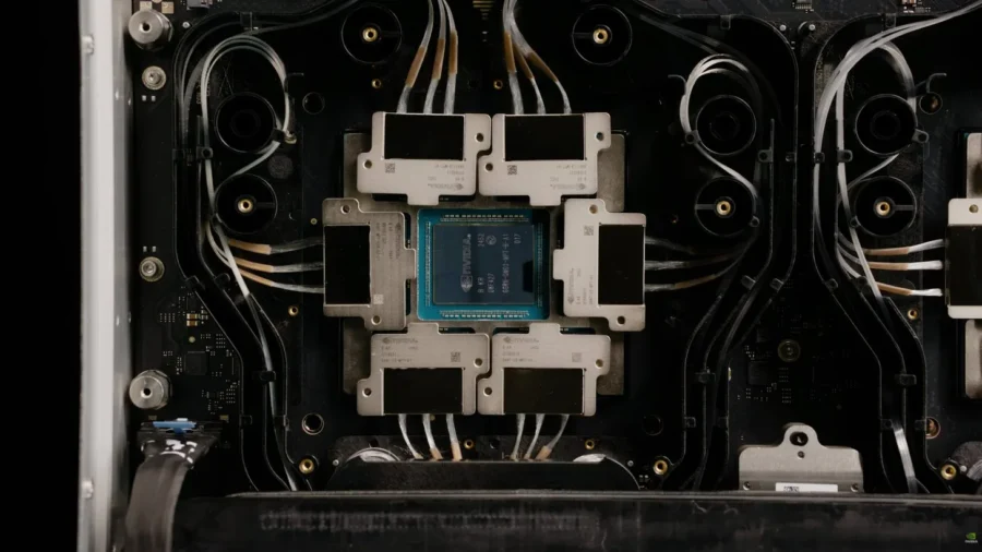
In NVIDIA’s new road map, CPO, together with the Feynman GPU family, is placed at the connection layer at the center of artificial intelligence factories. This technology provides higher bandwidth, lower latency and more efficient data transfer between accelerators such as GPU and CPU. Especially in systems where hundreds or thousands of GPUs work together, connection architecture has now become as critical a topic as processing power.
Under normal circumstances, CPO technology was expected to become widespread on a commercial scale around 2033. With NVIDIA bringing forward the calendar, this transition was moved to 2028. This date coincides with the release period of the Feynman GPU family. In addition to Feynman GPUs, the company’s 2028 platform will include components such as Rosa CPU, BlueField-5, NVLink 8 CPO, Spectrum 7 204T and CX10. The Feynman GPU family stands out not only with CPO but also with innovations in packaging and memory.
3D Die Stacking technology for Feynman was included in the GTC 2026 road map. This points to a new packaging approach based on vertical stacking of GPU dies. In the same road map, the special HBM expression was used for Feynman instead of the standard HBM. While there is HBM4 in the Rubin family and HBM4E in Rubin Ultra, a more customized HBM solution is on the agenda on the Feynman side. NVIDIA also has a new name on the data center CPU side.
The Feynman platform is positioned with Rosa CPU instead of Vera CPU. Rosa entered the roadmap as NVIDIA’s new data center CPU architecture prepared for the Feynman era. Therefore, the 2028 platform consists not only of the new GPU family, but also of a broader artificial intelligence system architecture in which GPU, CPU, network, DPU and optical connection components work together. The acceleration on the CPO side is not limited to NVIDIA alone.
AMD, Broadcom, Meta, Microsoft, NVIDIA and OpenAI were among the founding members of the Optical Compute Interconnect Multi-Source Agreement group, which was established in March 2026. This framework was established to create an open and interoperable optical connectivity standard for AI scaling systems. The technical framework includes NRZ modulation, WDM optical technology and the transition from module-centered structure to silicon-centered connection model.
The race in the industry is also progressing on the AMD side. It is stated that AMD is working with GlobalFoundries on the CPO side for the Instinct MI500 family, and will bring optical connection to the next generation accelerators through the photonic integrated circuit production and packaging process. This table shows that the competition for artificial intelligence accelerators in 2028 will not be limited to GPU cores or memory capacity.
Connection architecture, power efficiency and scalability become direct areas of competition. That’s why NVIDIA’s Feynman move is important. The company makes optical connection, as well as copper connection, the main design element in artificial intelligence data centers. The combination of Feynman GPU, Rosa CPU and NVLink 8 CPO will be a new transition point in NVIDIA’s AI hardware architecture in 2028. This transition is gearing up for next-generation AI systems that require larger GPU clusters, denser data transfer, and lower connection latency.


Comments
You can write your views about this story. Comments may be moderated according to site settings.